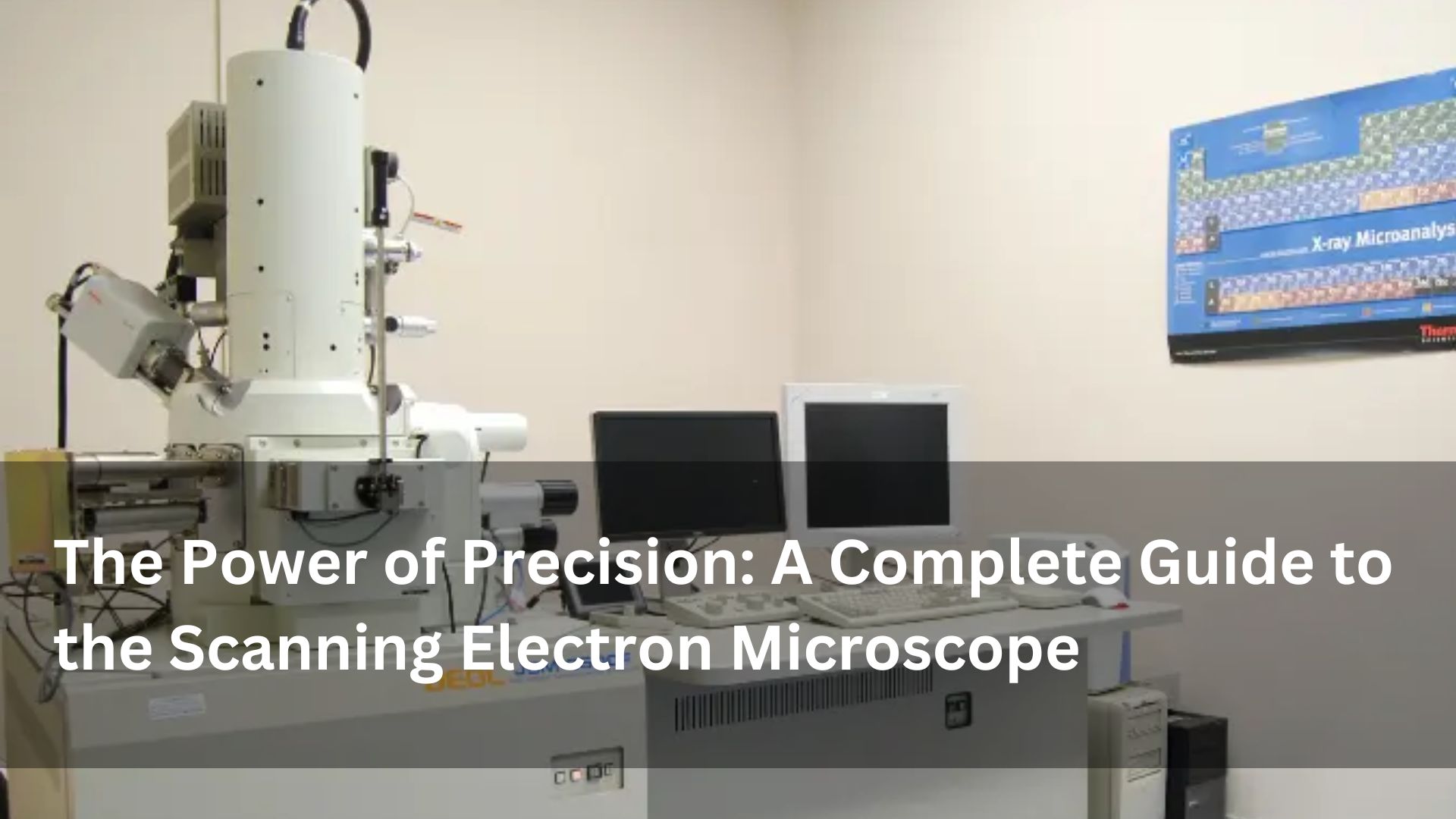
In the world of scientific imaging, the scanning electron microscope (SEM) is a game-changing instrument. Unlike optical microscopes, which use visible light to magnify images, the scanning electron microscope uses a focused beam of electrons. This allows it to achieve far greater resolution, revealing fine surface details of specimens that are invisible to the naked eye. From biological tissues and nanoparticles to semiconductors and metals, SEM has become indispensable in research, development, and quality assurance. This guide explores everything you need to know about the scanning electron microscope—how it works, why it matters, and where it’s heading.
What is a Scanning Electron Microscope?
A scanning electron microscope is a type of electron microscope that creates images of a sample by scanning it with a focused beam of electrons. These electrons interact with the atoms in the sample, producing various signals that can be detected and used to form an image. SEMs are renowned for their ability to produce high-resolution, three-dimensional-like images of a sample’s surface topography.
How Does a Scanning Electron Microscope Work?
The working principle of a scanning electron microscope involves several core components:
Electron Gun: Emits a stream of high-energy electrons.
Electromagnetic Lenses: Focus the electron beam into a fine spot.
Scanning Coils: Move the beam in a raster pattern over the sample surface.
Detectors: Capture secondary electrons, backscattered electrons, and X-rays emitted from the sample.
Image Processor: Converts signals into a high-contrast image.
The electrons interact with the sample in different ways, creating secondary and backscattered electrons that carry information about the sample’s surface and composition.
Key Components of a Scanning Electron Microscope
Each scanning electron microscope is built from several essential components:
Vacuum Chamber: Maintains a vacuum to allow electron travel.
Specimen Stage: Holds and manipulates the sample.
Control Console: Allows users to adjust focus, magnification, and scan speed.
Display Monitor: Shows real-time images of the sample.
These components work together seamlessly to ensure precise imaging and accurate data collection.
Applications of the Scanning Electron Microscope
The versatility of the scanning electron microscope means it’s used in a wide range of industries and fields:
Biology and Medicine: Studying cells, tissues, and microorganisms.
Materials Science: Analyzing the microstructure of metals, ceramics, and polymers.
Semiconductors: Inspecting microchips and integrated circuits.
Forensics: Identifying gunshot residue, fibers, and other trace evidence.
Geology: Examining mineral and rock textures.
In each of these areas, the SEM provides high-resolution insights that are essential for analysis, diagnostics, and innovation.
Advantages of Using a Scanning Electron Microscope
There are numerous benefits to using a scanning electron microscope:
High Resolution: Capable of resolving features as small as 1 nanometer.
Depth of Field: Produces images with excellent depth and surface detail.
Elemental Analysis: Equipped with EDX (Energy Dispersive X-ray Spectroscopy) for chemical composition analysis.
3D Surface Topography: Provides pseudo-3D images for surface mapping.
Non-Destructive Testing: Allows repeated scanning of the same area.
These features make SEM an essential tool for precision imaging.
Limitations and Challenges of the Scanning Electron Microscope
Despite its advantages, the scanning electron microscope has limitations:
High Cost: Equipment and maintenance can be expensive.
Sample Preparation: Non-conductive samples require coating with a conductive material.
Vacuum Requirement: Samples must be stable in a vacuum environment.
Complex Operation: Requires trained personnel to operate and interpret results.
Understanding these limitations helps users make informed decisions about SEM use.
Types of Scanning Electron Microscopes
There are several types of scanning electron microscopes designed for specific applications:
Conventional SEM: Most common, for general imaging tasks.
Environmental SEM (ESEM): Allows imaging of wet or non-conductive samples.
Field Emission SEM (FE-SEM): Offers higher resolution using a field emission source.
Low Vacuum SEM: Suitable for biological and soft materials.
Choosing the right SEM depends on the imaging needs and sample type.
Recent Innovations in Scanning Electron Microscope Technology
Technological advancements have led to significant improvements in scanning electron microscope capabilities:
Automation: Reduced operator dependency and faster throughput.
Improved Detectors: Better signal capture for low-voltage imaging.
AI Integration: Automated feature recognition and analysis.
Compact Designs: Benchtop SEMs for education and small labs.
These innovations are making SEMs more accessible and powerful than ever.
Conclusion
The scanning electron microscope is a cornerstone of modern scientific research and industrial inspection. Its unmatched resolution, depth of field, and versatility make it indispensable for detailed imaging and analysis. As technology evolves, the SEM continues to break new ground in microscopy, expanding its role in diagnostics, materials science, and beyond. For researchers, engineers, and manufacturers, investing in a scanning electron microscope is not just about seeing smaller—it’s about seeing more accurately, more effectively, and more intelligently.


